CY6117A
CY6117A is 2K x 8 Static RAM manufactured by Cypress.
Features
D D D D D D D
Automatic powerĆdown when deselected CMOS for optimum speed/power High speed Ċ 20 ns Low active power Ċ 550 m W Low standby power Ċ 110 m W TTLĆpatible inputs and outputs Capable of withstanding greater than 2001V electrostatic discharge
The CY6116A and CY6117A are highĆ performance CMOS static RAMs orgaĆ nized as 2048 words by 8 bits. Easy memoryexpansionisprovidedbyanactive LOW chip enable (CE) and active LOW output enable (OE), and threeĆstate drivĆ ers. The CY6116A and CY6117A have an automatic powerĆdown feature
, reducing the power consumption by 83% when deĆ selected. Writingtothedeviceisacplishedwhen the chip enable (CE) and write enable (WE) inputs are both LOW. Data on the I/Opins(I/O0 through I/O7)iswritteninto
Functional Description the memory location specified on the adĆ dress pins (A0 through A10). ReadingthedeviceisacplishedbytakĆ ing chip enable (CE) and output enable (OE) LOW while write enable (WE) reĆ mains HIGH.Undertheseconditions,the contents of the memory location specified on the address pins will appear on the I/O pins. The I/O pins remain in highĆimpedance state when chip enable (CE) is HIGH or write enable (WE) is LOW. The CY6116A and CY6117A utilize a die coat to insure alpha immunity.
2K x 8 Static RAM
CY6116A CY6117A
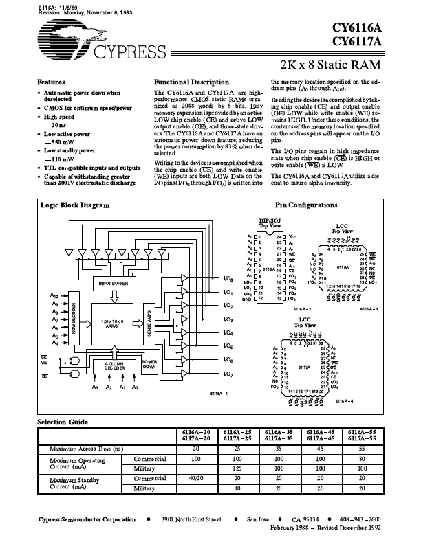
Logic Block Diagram
A7 A6 A5 A4 A3 A2 A1 1 2 3 4 5 6 7 8 9 10 11 12 6116A
Pin Configurations
DIP/SOJ Top View
24 23 22 21 20 19 18 17 16 15 14 13 VCC A8 A9 WE OE A10 CE I/O7 I/O6 I/O5 I/O4 I/O3 A3 A2 NC NC A1 A0 I/O0 5 6 7 8 9 10 11 6116A 4 A4 A7 V CC
LCC Top View
A8 3 2 1 28 27 26 25 24 23 22 21 20 19 1213 14 151617 18 1 I/O 2 GND I/O 3 I/O 4 I/O 5 I/O 6 WE OE A10 NC NC CE I/O7 A9 6116A-3 A5 A6
I/O0
INPUT BUFFER
A0 I/O0 I/O1
GND ROW DECODER
A9 A8 A7 A6 A5 A4
I/O2
SENSE AMPS
6116A-2
128 x 16 x 8 ARRAY
I/O3
I/O5
4 A6 A5 A4 A3 A2 5 6 7 8 9 10 11 12 13
1 32 31 30 29 28 27 26 A8 A9 NC WE OE A10 CE I/O7 I/O6
CE WE COLUMN DECODER OE POWER DOWN
I/O6
6117A
I/O7
A1...