CY62128V18
Features
- Low voltage range:
- 2.7V- 3.6V (CY62128V)
- 2.3V- 2.7V (CY62128V25)
- -
- -
- - 1.6V- 2.0V (CY62128V18) Low active power and standby power Easy memory expansion with CE and OE features
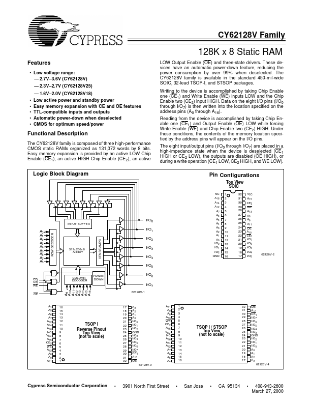
TTL-patible inputs and outputs Automatic power-down when deselected CMOS for optimum speed/power LOW Output Enable (OE) and three-state drivers. These devices have an automatic power-down feature
, reducing the power consumption by over 99% when deselected. The CY62128V family is available in the standard 450-mil-wide SOIC, 32-lead TSOP-I, and STSOP packages. Writing to the device is acplished by taking Chip Enable one (CE1) and Write Enable (WE) inputs LOW and the Chip Enable two (CE2) input HIGH. Data on the eight I/O pins (I/O0 through I/O 7) is then written into the location specified on the address pins (A 0 through A16). Reading from the device is acplished by taking Chip Enable one (CE1) and Output Enable (OE) LOW while forcing Write Enable (WE) and Chip Enable two (CE2) HIGH. Under these...