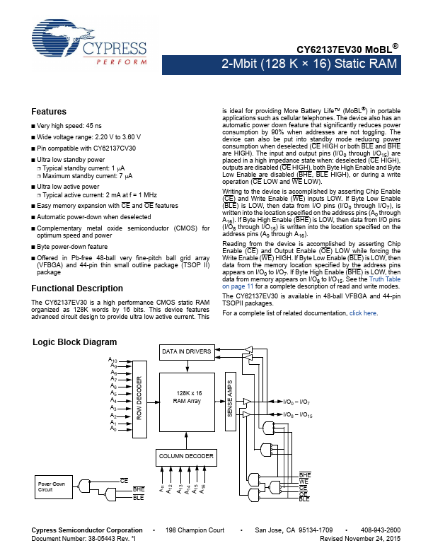
• Part: CY62137EV30
  • Description: 2-Mbit (128K x 16) Static RAM
  • Manufacturer: Cypress
  • Size: 578.36 KB
Download CY62137EV30 Datasheet PDF
Cypress
CY62137EV30
CY62137EV30 is 2-Mbit (128K x 16) Static RAM manufactured by Cypress.
CY62137EV30 Mo BL® 2-Mbit (128 K × 16) Static RAM 2-Mbit (128 K × 16) Static RAM Features - Very high speed: 45 ns - Wide voltage range: 2.20 V to 3.60 V - Pin patible with CY62137CV30 - Ultra low standby power - Typical standby current: 1 A - Maximum standby current: 7 A - Ultra low active power - Typical active current: 2 m A at f = 1 MHz - Easy memory expansion with CE and OE Features - Automatic power-down when deselected - plementary metal oxide semiconductor (CMOS) for optimum speed and power - Byte power-down feature - Offered in Pb-free 48-ball very fine-pitch ball grid array (VFBGA) and 44-pin thin small outline package (TSOP II) package Functional Description The CY62137EV30 is a high performance CMOS static RAM organized as 128K words by 16 bits. This device Features advanced circuit design to provide ultra low active current. This is ideal for providing More Battery Life™ (Mo BL®) in portable applications such as cellular telephones. The device also has an automatic power down feature that significantly reduces power consumption by 90% when addresses are not toggling. The device can also be put into standby mode reducing power consumption when deselected (CE HIGH or both BLE and BHE are HIGH). The input and output pins (I/O0 through I/O15) are placed in a high impedance state when: deselected (CE HIGH), outputs are disabled (OE HIGH), both Byte High Enable and Byte Low Enable are disabled (BHE, BLE HIGH), or during a write operation (CE LOW and WE LOW). Writing to the device is acplished by asserting Chip Enable (CE) and Write Enable (WE) inputs LOW. If Byte Low Enable (BLE) is LOW, then data from I/O pins (I/O0 through I/O7), is written into the location specified on the address pins (A0 through A16). If Byte High Enable (BHE) is LOW, then data from I/O pins (I/O8 through I/O15) is written into the location specified on the address pins (A0 through A16). Reading from the device is acplished by asserting Chip Enable (CE) and Output Enable...