CY62146VLL-70ZI
Overview
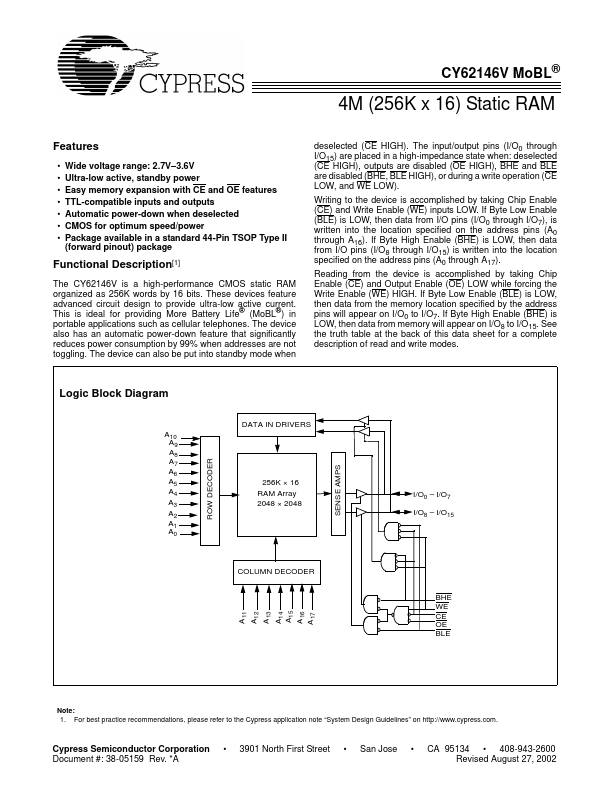
- Wide voltage range: 2.7V-3.6V Ultra-low active, standby power Easy memory expansion with CE and OE features TTL-compatible inputs and outputs Automatic power-down when deselected CMOS for optimum speed/power Package available in a standard 44-Pin TSOP Type II (forward pinout) package deselected (CE HIGH). The input/output pins (I/O0 through I/O15) are placed in a high-impedance state when: deselected (CE HIGH), outputs are disabled (OE HIGH), BHE and BLE are disabled (BHE, BLE HIGH), or during a write operation (CE LOW, and WE LOW). Writing to the device is accomplished by taking Chip Enable (CE) and Write Enable (WE) inputs LOW. If Byte Low Enable (BLE) is LOW, then data from I/O pins (I/O0 through I/O7), is written into the location specified on the address pins (A0 through A16). If Byte High Enable (BHE) is LOW, then data from I/O pins (I/O8 through I/O15) is written into the location specified on the address pins (A0 through A17). Reading from the device is accomplished by taking Chip Enable (CE) and Output Enable (OE) LOW while forcing the Write Enable (WE) HIGH. If Byte Low Enable (BLE) is LOW, then data from the memory location specified by the address pins will appear on I/O0 to I/O7. If Byte High Enable (BHE) is LOW, then data from memory will appear on I/O8 to I/O15. See the truth table at the back of this data sheet for a complete description of read and write modes. Functional Description[1] The CY62146V is a high-performance CMOS static RAM organized as 256K words by 16 bits. These devices feature advanced circuit design to provide ultra-low active current. This is ideal for providing More Battery Life® (MoBL®) in portable applications such as cellular telephones. The device also has an automatic power-down feature that significantly reduces power consumption by 99% when addresses are not toggling. The device can also be put into standby mode when Logic Block Diagram D