CY62157CV33
Overview
- High speed - 55 ns and 70 ns availability
- Voltage range: - CY62157CV25: 2.2V-2.7V - CY62157CV30: 2.7V-3.3V - CY62157CV33: 3.0V-3.6V
- Ultra-low active power - Typical active current: 1.5 mA @ f = 1 MHz * * *
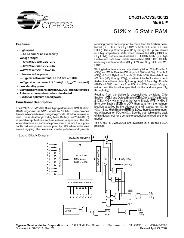
- - Typical active current: 5.5 mA @ f = fmax (70 ns speed) Low standby power Easy memory expansion with CE1, CE2 and OE features Automatic power-down when deselected CMOS for optimum speed/power reducing power consumption by more than 99% when deselected (CE1 HIGH or CE2 LOW or both BLE and BHE are HIGH). The input/output pins (I/O0 through I/O15) are placed in a high-impedance state when: deselected (CE1 HIGH or CE2 LOW), outputs are disabled (OE HIGH), both Byte High Enable and Byte Low Enable are disabled (BHE, BLE HIGH), or during a write operation (CE1 LOW and CE2 HIGH and WE LOW). Writing to the device is accomplished by taking Chip Enable 1 (CE1) and Write Enable (WE) inputs LOW and Chip Enable 2 (CE2) HIGH. If Byte Low Enable (BLE) is LOW, then data from I/O pins (I/O0 through I/O7), is written into the location specified on the address pins (A0 through A18). If Byte High Enable (BHE) is LOW, then data from I/O pins (I/O8 through I/O15) is written into the location specified on the address pins (A0 through A18). Reading from the device is accomplished by taking Chip Enable 1 (CE1) and Output Enable (OE) LOW and Chip Enable 2 (CE2) HIGH while forcing the Write Enable (WE) HIGH. If Byte Low Enable (BLE) is LOW, then data from the memory location specified by the address pins will appear on I/O0 to I/O7. If Byte High Enable (BHE) is LOW, then data from memory will appear on I/O8 to I/O15. See the truth table at the back of this data sheet for a complete description of read and write modes. The CY62157CV25/30/33 are available in a 48-ball FBGA package. Functional Description The CY62157CV25/30/33 are high-performance CMOS static RAMs organized as 512K words by 16 b