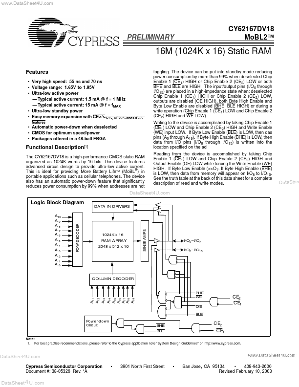
CY62167DV18
CY62167DV18 is 16M (1024K x 16) Static RAM manufactured by Cypress.
..
PRELIMINARY
CY62167DV18 Mo BL2™
16M (1024K x 16) Static RAM
Features
- Very high speed: 55 ns and 70 ns
- Voltage range: 1.65V to 1.95V
- Ultra-low active power
- Typical active current: 1.5 m A @ f = 1 MHz
- Typical active current: 15 m A @ f = f MAX
- Ultra-low standby power
- Easy memory expansion with CE</>1</>, CE2</> and OE</>
Features toggling. The device can be put into standby mode reducing power consumption by more than 99% when deselected Chip Enable 1 (CE1) HIGH or Chip Enable 2 (CE2) LOW or both BHE and BLE are HIGH. The input/output pins (I/O0 through I/O15) are placed in a high-impedance state when: deselected Chip Enable 1 (CE1) HIGH or Chip Enable 2 (CE2) LOW, outputs are disabled (OE HIGH), both Byte High Enable and Byte Low Enable are disabled (BHE, BLE HIGH) or during a write operation (Chip Enable 1 (CE1) LOW and Chip Enable 2 (CE2) HIGH and WE LOW). Writing to the device is acplished by taking Chip Enable 1 (CE1) LOW and Chip Enable 2 (CE2) HIGH and Write Enable (WE) input LOW. If Byte Low Enable (BLE) is LOW, then das pins (A0 through A19). If Byte High Enable (BHE) is LOW, then data from I/O pins (I/O8 through I/O15) is written into the location specified on the ad Reading from the device is acplished by taking Chip Enable 1 (CE1) LOW and Chip Enable 2 (CE2) HIGH and Output Enable (OE) LOW while forcing the Write Enable (WE) HIGH. If Byte Low Enable (<>O7. If Byte High Enable (BHE) is LOW, then data from memory will appear on I/O8 to I/O15. See the truth table at the back of this data sheet for a plete description of read and write modes.
- Automatic power-down when deselected
- CMOS for optimum speed/power
- Packages offered in a 48-ball FBGA
Functional Description[1]
The CY62167DV18 is a high-performance CMOS static RAM organized as 1024K words by 16 bits. This device Features advanced circuit design to provide ultra-low active current. This is ideal for providing More Battery Life (Mo BL®) in portable...