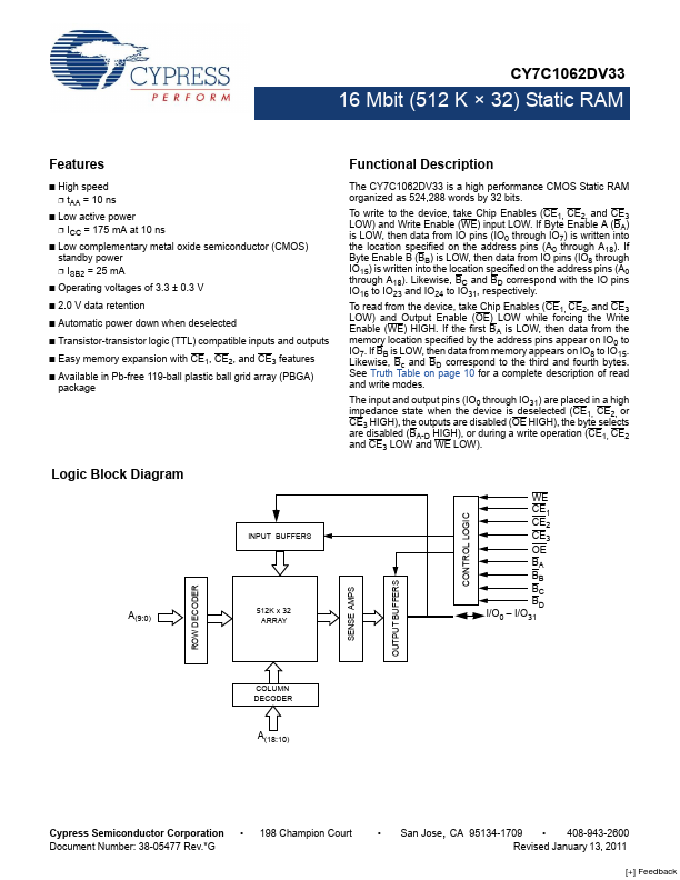
• Part: CY7C1062DV33
  • Description: 16 Mbit (512K x 32) Static RAM
  • Manufacturer: Cypress
  • Size: 381.80 KB
Download CY7C1062DV33 Datasheet PDF
Cypress
CY7C1062DV33
CY7C1062DV33 is 16 Mbit (512K x 32) Static RAM manufactured by Cypress.
16 Mbit (512 K × 32) Static RAM Features - High speed - t AA = 10 ns - Low active power - ICC = 175 m A at 10 ns - Low plementary metal oxide semiconductor (CMOS) standby power - ISB2 = 25 m A - Operating voltages of 3.3 ± 0.3 V - 2.0 V data retention - Automatic power down when deselected - Transistor-transistor logic (TTL) patible inputs and outputs - Easy memory expansion with CE1, CE2, and CE3 Features - Available in Pb-free 119-ball plastic ball grid array (PBGA) package Logic Block Diagram INPUT BUFFERS A(9:0) 512K x 32 ARRAY Functional Description The CY7C1062DV33 is a high performance CMOS Static RAM organized as 524,288 words by 32 bits. To write to the device, take Chip Enables (CE1, CE2, and CE3 LOW) and Write Enable (WE) input LOW. If Byte Enable A (BA) is LOW, then data from IO pins (IO0 through IO7) is written into the location specified on the address pins (A0 through A18). If Byte Enable B (BB) is LOW, then data from IO pins (IO8 through IO15) is written into the location specified on the address pins (A0 through A18). Likewise, BC and BD correspond with the IO pins IO16 to IO23 and IO24 to IO31, respectively. To read from the device, take Chip Enables (CE1, CE2, and CE3 LOW) and Output Enable (OE) LOW while forcing the Write Enable (WE) HIGH. If the first BA is LOW, then data from the memory location specified by the address pins appear on IO0 to IO7. If BB is LOW, then data from memory appears on IO8 to IO15. Likewise, Bc and BD correspond to the third and fourth bytes. See Truth Table on page 10 for a plete description of read and write modes. The input and output pins (IO0 through IO31) are placed in a high impedance state when the device is deselected (CE1, CE2, or CE3 HIGH), the outputs are disabled (OE HIGH), the byte selects are disabled (BA-D HIGH), or during a write operation (CE1, CE2 and CE3 LOW and WE LOW). WE CE1 CE2 CE3 OE BA BB BC BD I/O0 - I/O31 ROW DECODER SENSE AMPS OUTPUT BUFFERS CONTROL LOGIC COLUMN...