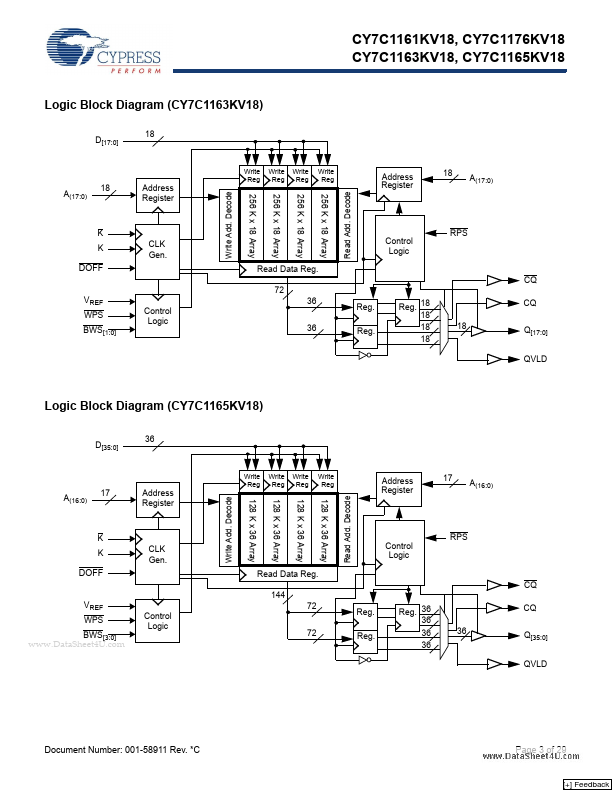
CY7C1163KV18 Description
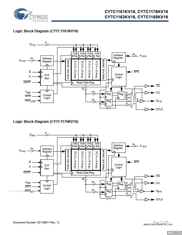
Similar to QDR II architecture, QDR II+ architecture consists of two separate ports: the read port and the write port to access the memory array. The read port has dedicated data outputs to support read operations and the write port has dedicated data inputs to support write operations.
CY7C1163KV18 Key Features
- 2 M x 8 CY7C1176KV18
- 2 M x 9 CY7C1163KV18
- 1 M x 18 CY7C1165KV18
- 512 K x 36
- Supports concurrent transactions 550-MHz clock for high bandwidth Four-word burst for reducing address bus frequency Dou
- Supports both 1.5 V and 1.8 V I/O supply HSTL inputs and variable drive HSTL output buffers Available in 165-ball FBGA p
- Functional Description