Datasheet4U Logo Datasheet4U.com
Cypress (now Infineon) logo

CY7C11651KV18 Datasheet

Manufacturer: Cypress (now Infineon)
CY7C11651KV18 datasheet preview

CY7C11651KV18 Details

Part number CY7C11651KV18
Datasheet CY7C11651KV18 CY7C11611KV18 Datasheet (PDF)
File Size 918.04 KB
Manufacturer Cypress (now Infineon)
Description 18-Mbit QDR II SRAM 4-Word Burst Architecture
CY7C11651KV18 page 2 CY7C11651KV18 page 3

CY7C11651KV18 Overview

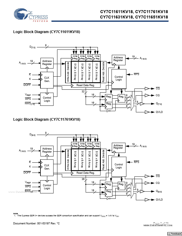
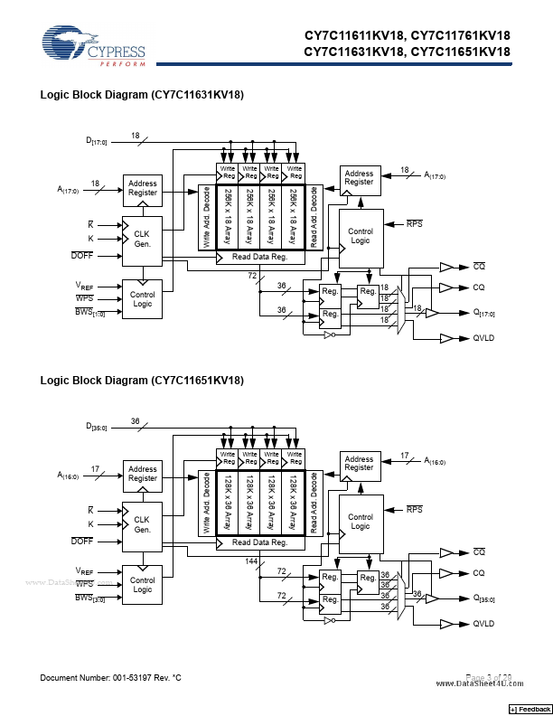
Similar to QDR II architecture, QDR II+ architecture consists of two separate ports: the read port and the write port to access the memory array. The read port has dedicated data outputs to support read operations and the write port has dedicated data inputs to support write operations.

CY7C11651KV18 Key Features

  • Supports concurrent transactions 550 MHz clock for high bandwidth 4-word burst for reducing address bus frequency Double
  • SRAM uses rising edges only Echo clocks (CQ and CQ) simplify data capture in high speed systems Data valid pin (QVLD) to

CY7C11651KV18 Distributor

Cypress (now Infineon) Datasheets

More from Cypress (now Infineon)

Datasheet4U Logo
Since 2006. D4U Semicon. About Datasheet4U Contact Us Privacy Policy Purchase of parts