CY7C1318JV18 Description
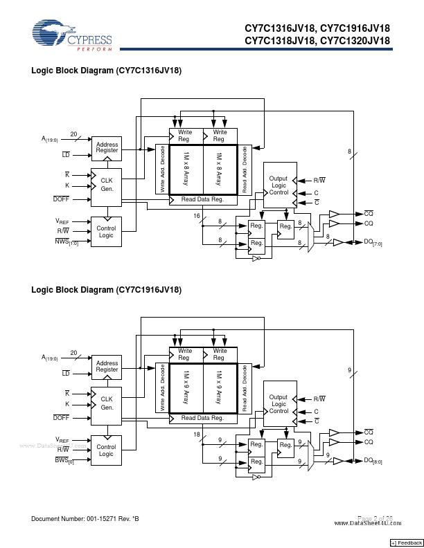
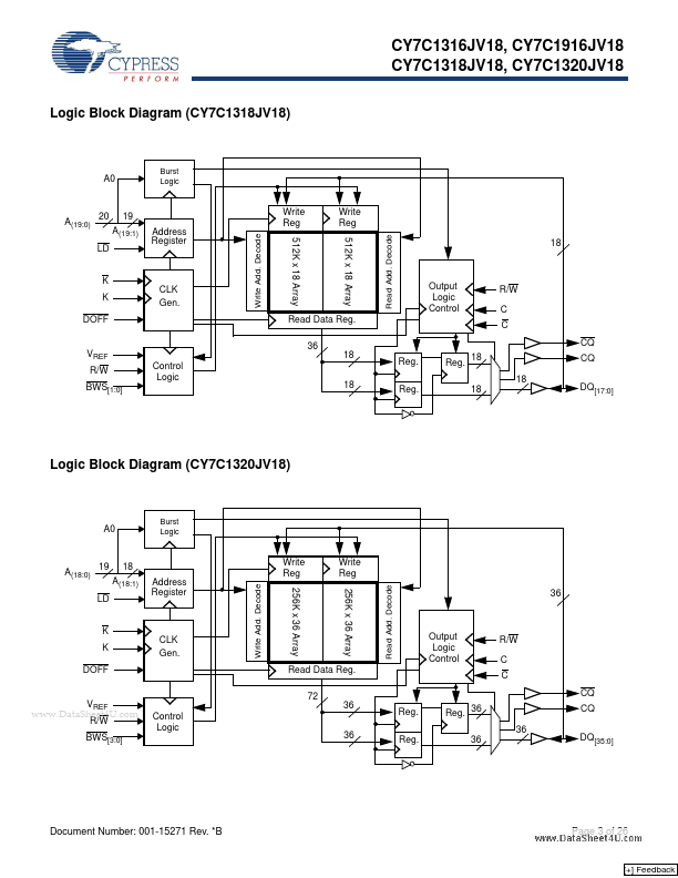
The DDR-II consists of an SRAM core with advanced synchronous peripheral circuitry and a one-bit burst counter. Addresses for read and write are latched on alternate rising edges of the input (K) clock. Write data is registered on the rising edges of both K.
CY7C1318JV18 Key Features
- 2M x 8 CY7C1916JV18
- 2M x 9 CY7C1318JV18
- 1M x 18 CY7C1320JV18
- 512K x 36