CY7C1318KV18
Description
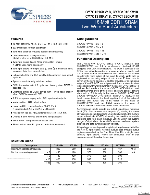
Maximum operating frequency Maximum operating current ×8 ×9 × 18 × 36 333 MHz 333 440 440 450 560 300 MHz 300 420 420 430 520 250 MHz 250 370 370 380 460 200 MHz 200 330 330 340 400 167 MHz 167 300 300 310 360 Unit MHz mA. Cypress Semiconductor Corporation Document Number: 001-58905 Rev.