CY7C1483V25 Description
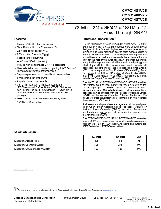
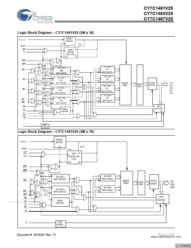
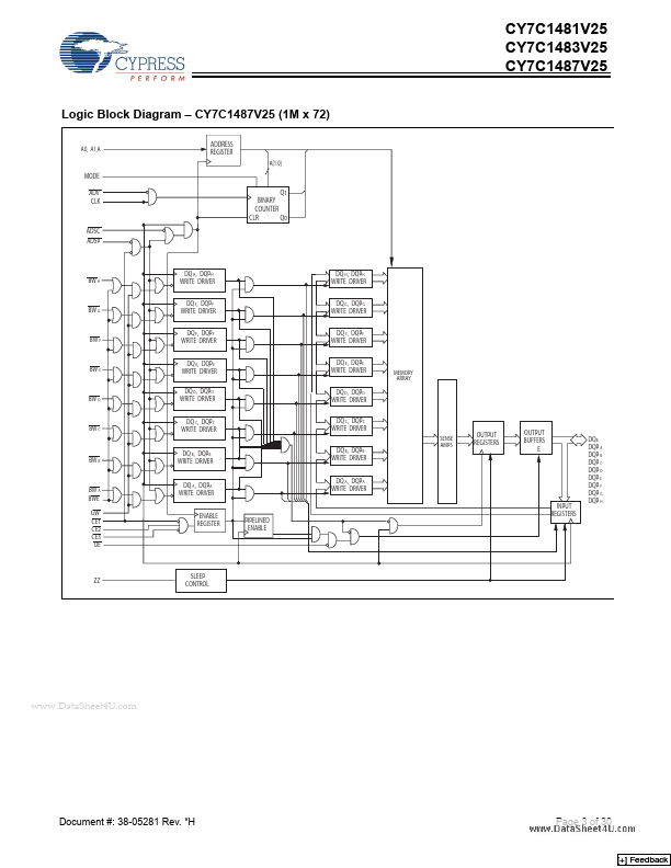
Maximum access delay from clock rise is 6.5 ns (133-MHz version). A 2-bit on-chip counter captures the first address in a burst and increments the address automatically for the rest of the burst access. All synchronous inputs are gated by registers controlled by a positive edge triggered Clock Input (CLK).
CY7C1483V25 Key Features
- 6.5 ns (133-MHz version)
- Provide high-performance 2-1-1-1 access rate
- User selectable burst counter supporting Intel® Pentium® interleaved or linear burst sequences
- Separate processor and controller address strobes
- Synchronous self timed write
- Asynchronous output enable
- IEEE 1149.1 JTAG-patible Boundary Scan
- 198 Champion Court
- San Jose, CA 95134-1709