IMIC9531
Features
Features
- Dedicated clock buffer power pins for reduced noise, crosstalk and jitter
- Input clock frequency of 25 MHz to 33 MHz
- Output frequencies of XINx1, XINx2, XINx3 and XINx4
- One output bank of 5 clocks.
- One REF XIN clock output.
- SMBus clock control interface for individual clock disabling and SSCG control
- Output clock duty cycle is 50% (± 5%)
- < 250 ps skew between output clocks within a bank
- Output jitter <175 ps
- Spread Spectrum feature for reduced electromagnetic interference (EMI)
- OE pin for entire output bank enable control and testability
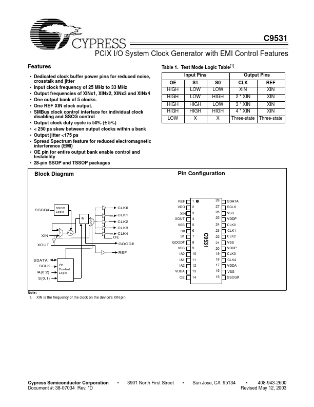
- 28-pin SSOP and TSSOP packages Table 1. Test Mode Logic Table[1] Input Pins OE HIGH HIGH HIGH HIGH LOW S1 LOW LOW HIGH HIGH X S0 LOW HIGH LOW HIGH X Output Pins CLK XIN 2
- XIN 3
- XIN 4
- XIN REF XIN XIN XIN XIN
Three-state Three-state
Block Diagram
Pin Configuration
1 2 3 4 5 6
28 27 26 25 24 23
SDATA SCLK VSS VDDP CLK0 CLK1 CLK2 VSS VDDP CLK3 CLK4 VDDA VSS SSCG#
SSCG#
SSCG Logic /N
1 0
CLK0...