W152
Features
- Spread Aware™- designed to work with SSFTG reference signals
- Two banks of four outputs each
- Configuration options to halve, double, or quadruple the reference frequency refer to Table 1 to determine the specific option which meets your multiplication needs
- Outputs may be three-stated
- Available in 16-pin SOIC package
- Extra strength output drive available (-11/-12 versions)
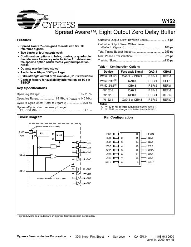
- Contact factory for availability information on 16-pin TSSOP Output to Output Skew: Between Banks 215 ps Output to Output Skew: Within Banks (Refer to Figure 4) 100 ps Total Timing Budget Impact: 555 ps Max. Phase Error Variation: ±225 ps Tracking Skew: ±130 ps Table 1. Configuration Options Device W152-1/11 W152-2/12 W152-3 W152-3 W152-4
[1]
Feedback Signal QA0:3 or QB0:3 QA0:3 QB0:3...