W194
Features
- Two outputs
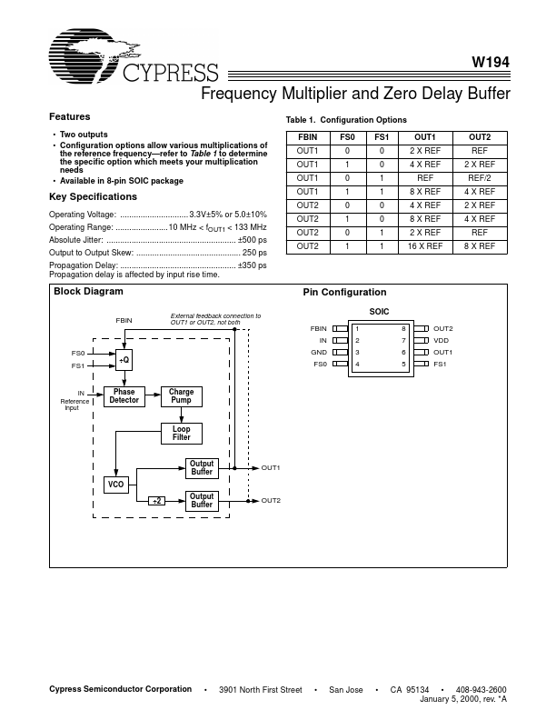
- Configuration options allow various multiplications of the reference frequency- refer to Table 1 to determine the specific option which meets your multiplication needs
- Available in 8-pin SOIC package Table 1. Configuration Options FBIN OUT1 OUT1 OUT1 OUT1 OUT2 Operating Voltage: 3.3V±5% or 5.0±10% Operating Range: 10 MHz < f OUT1 < 133 MHz Absolute Jitter: ±500 ps Output to Output Skew: 250 ps Propagation Delay: ±350 ps Propagation delay is affected by input rise time. OUT2 OUT2 OUT2 FS0 0 1 0 1 0 1 0 1 FS1 0 0 1 1 0 0 1 1 OUT1 2 X REF 4 X REF REF 8 X REF 4 X REF 8 X REF 2 X REF 16 X REF OUT2 REF 2 X REF REF/2 4 X REF 2 X REF 4 X REF REF 8 X REF
Key Specifications
Block Diagram
FBIN
External feedback connection to OUT1 or OUT2, not both
Pin...