W232
Key Features
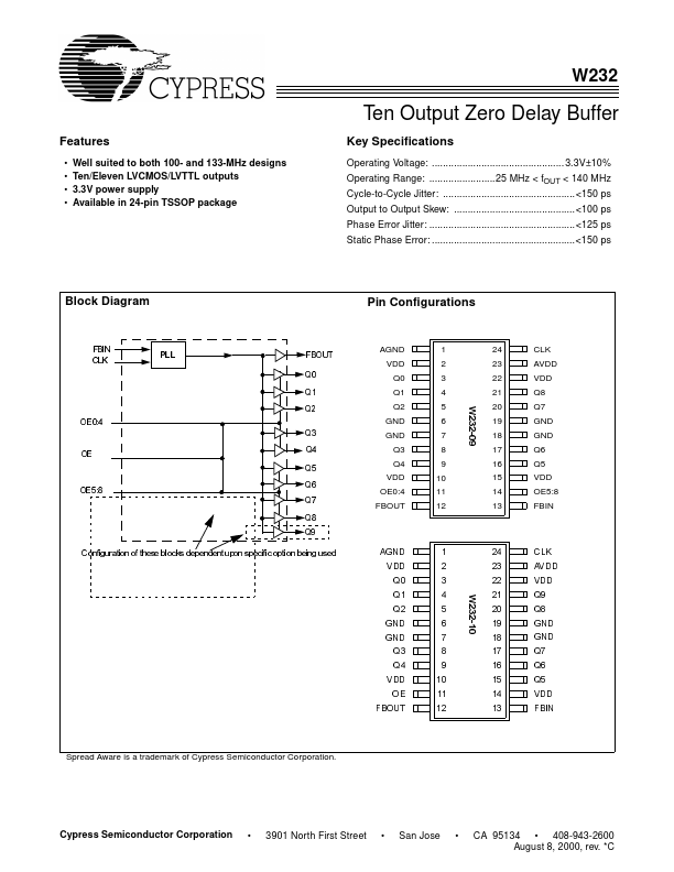
- Well suited to both 100- and 133-MHz designs Ten/Eleven LVCMOS/LVTTL outputs 3.3V power supply Available in 24-pin TSSOP package
- 3901 North First Street
| Part Number | Manufacturer | Description |
|---|---|---|
| KDC-W237 | Kenwood | CD RECEIVER INSTRUCTION MANUAL |
| KDC-W237GY | Kenwood | CD RECEIVER SERVICE MANUAL |
| KDC-W237AY | Kenwood | CD RECEIVER SERVICE MANUAL |
| W236 | VBsemi | Dual N-Channel 20V MOSFET |