W40S11-23
Key Features
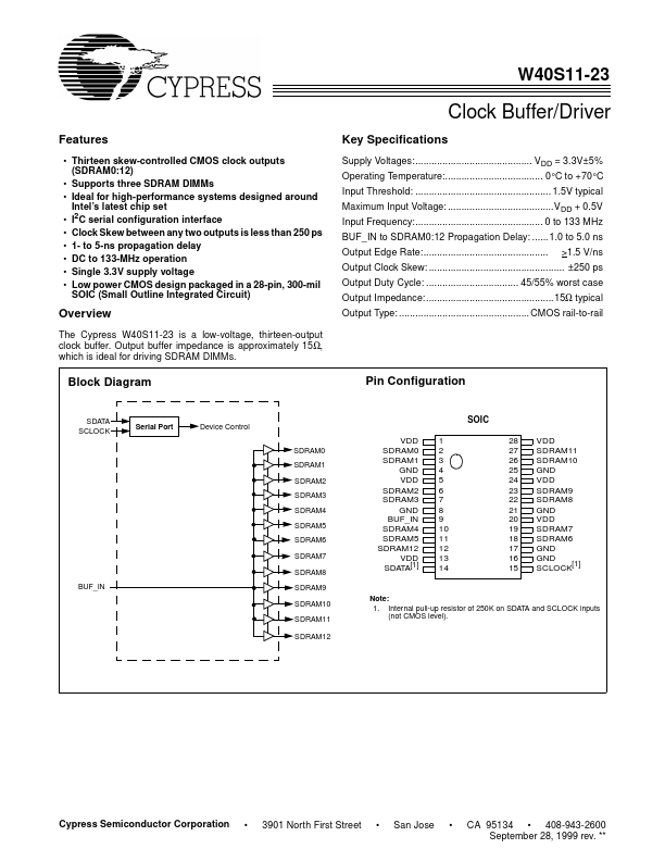
- Thirteen skew-controlled CMOS clock outputs (SDRAM0:12)
- Supports three SDRAM DIMMs
- Ideal for high-performance systems designed around Intel’s latest chip set
- I2C serial configuration interface
- Clock Skew between any two outputs is less than 250 ps
- 1- to 5-ns propagation delay
- DC to 133-MHz operation
- Single 3.3V supply voltage