CG7480AT
Key Features
- Temperature ranges ❐ -40 °C to 125 °C
- High speed ❐ tAA = 15 ns
- Low active power ❐ ICC = 120 mA at 67 MHz
- Low CMOS standby power ❐ ISB2 = 20 mA
- 2.0-V data retention
- Automatic power-down when deselected
- Transistor-transistor logic (TTL)-compatible inputs and outputs
- Easy memory expansion with CE and OE features
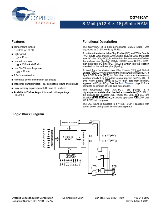
- Available in Pb-free 44-pin thin small outline package (TSOP) II. Functional Description The CG7480AT is a high performance CMOS Static RAM organized as 512 K words by 16 bits. To write to the device, take Chip Enable (CE) and Write Enable (WE) inputs LOW. If Byte LOW Enable (BLE) is LOW, then data from I/O pins (I/O0-I/O7), is written into the location specified on the address pins (A0-A18). If Byte HIGH Enable (BHE) is LOW, then data from I/O pins (I/O8-I/O15) is written into the location specified on the address pins (A0-A18). To read from the device, take Chip Enable (CE) and Output Enable (OE) LOW while forcing the Write Enable (WE) HIGH. If Byte LOW Enable (BLE) is LOW, then data from the memory location specified by the address pins appears on I/O0-I/O7. If Byte HIGH Enable (BHE) is LOW, then data from memory appears on I/O8 to I/O15. See the Truth Table on page 11 for a complete description of read and write modes. The input/output pins (I/O0-I/O15) are placed in a high-impedance state when the device is deselected (CE HIGH), the outputs are disabled (OE HIGH), the BHE and BLE are disabled (BHE, BLE HIGH), or a write operation (CE LOW, and WE LOW) is in progress. The CG7480AT is available in a 44-pin TSOP II package with center power and ground (revolutionary) pinout. Logic Block Diagram