CY25823 Description
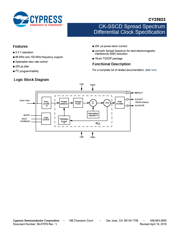
For a plete list of related documentation, click here. VDD VDDA Clock Input REFOUT Freq. Divider Phase Detector Charge Pump VCO Post Dividers M CLKOUT (SSCG Output) CLKOUT# SDATA SCLK PWRDWN Logic Control Feedback Divider N Modulating Waveform PLL VSS VSSA Cypress Semiconductor Corporation 198 Champion Court Document Number:.
CY25823 Key Features
- 3.3 V operation
- 96 MHz and 100 MHz frequency support
- Selectable slew rate control
- 200 ps jitter
- I2C programmability
- 250 A power-down current
- Lexmark Spread Spectrum for best electromagnetic
- 16-pin TSSOP package
- 198 Champion Court Document Number: 38-07579 Rev. -J
- San Jose, CA 95134-1709