S6BP401A Overview
Key Features
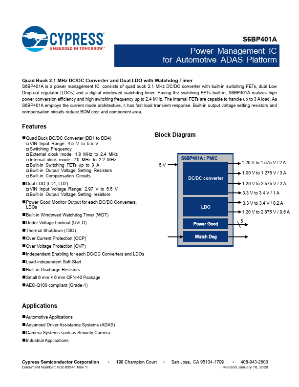
- Dual LDO (LD1, LD2) VIN Input Voltage Range: 2.97 V to 5.5 V Built-in Output Voltage Setting resistors
- Power Good Monitor Output for each DC/DC Converters, LDOs
- Built-in Windowed Watchdog Timer (WDT)
- Under Voltage Lockout (UVLO)
- Thermal Shutdown (TSD)
- Over Current Protection (OCP)
- Over Voltage Protection (OVP)
- Independent Enabling for each DC/DC Converters and LDOs
- Load-independent Soft-Start
- Built-in Discharge Resistors