Cypress Semiconductor W170-01
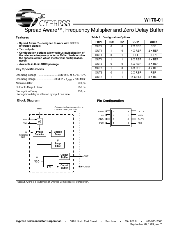
The W170-01 is a two-output zero delay buffer and frequency multiplier. It provides an external feedback path allowing maximum flexibility when implementing the Zero Delay feature. This is explained further in the sections of this data sheet titled “How to Implement Zero Delay,” and “Inserting Other Devices in Feedback Path.” The W170-01 is a pin-compatible upgrade of the Cypress W42C70-01.| Part No. | W170-01 |
|---|---|
| Datasheet | W170-01 Download |
| Manufacturer |  Cypress Semiconductor |
| Description | Spread Aware/ Frequency Multiplier and Zero Delay Buffer |
| Buy | Stock & Price |
FEATURES
● Spread Aware™—designed to work with SSFTG reference signals● Two outputs
● Configuration options allow various multiplication of the reference frequency, refer to Table 1 to determine the specific option which meets your multiplication needs
● Available in 8-pin SOIC package Table 1. Configuration Options FBIN OUT1 OUT1 OUT1 OUT1 OUT2 OUT2 OUT2 OUT2 FS0 0 1 0 1 0 1 0 1 FS1 0 0 1 1 0 0 1 1 OUT1 2 X REF 4 X REF REF 8 X REF 4 X REF 8 X REF 2 X REF 16 X REF OUT2 REF 2 X REF REF/2 4 X REF 2 X REF 4 X REF REF 8 X REF Key Specifications Operating Voltage: ...........................3.3V±5% or 5.0V± 10% Operating Range: .......................20 MHz < fOUT1 < 133 MHz Absolute Jitter: ......................................................... ±500 ps Output to Output Skew: .............................................. 250 ps Propagation Delay: ................................................... ±350 ps Propagation delay is affected by input rise time. Block Diagram FBIN External fee...

