Cypress Semiconductor W532
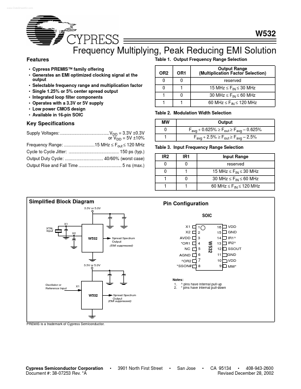
The W532 product is one of a series of devices in the Cypress PREMIS family. The PREMIS family incorporates the latest advances in PLL spread spectrum frequency synthesizer techniques. By frequency modulating the output with a low frequency carrier, peak EMI is greatly reduced.| Part No. | W532 |
|---|---|
| Datasheet | W532 Download |
| Manufacturer |  Cypress Semiconductor |
| Description | Peak Reducing EMI Solution |
| Buy | Stock & Price |
FEATURES
● Cypress PREMIS™ family offering● Generates an EMI optimized clocking signal at the output
● Selectable frequency range and multiplication factor
● Single 1.25% or 5% center spread output
● Integrated loop filter components
● Operates with a 3.3V or 5V supply
● Low power CMOS design
● Available in 16-pin SOIC Table 1. Output Frequency Range Selection OR2 0 0 1 1 OR1 0 1 0 1 Output Range (Multiplication Factor Selection) reserved 15 MHz ≤ FIN ≤ 30 MHz 30 MHz ≤ FIN ≤ 60 MHz 60 MHz ≤ FIN ≤ 120 MHz Table 2. Modulation Width Selection MW 0 1 Output Favg + 0.625% ≥ Fout ≥ Favg – 0.625% Favg + 2.5% ≥ Fout ≥ Favg – 2.5% Key Specifications Supply Voltages: ........................................VDD = 3.3V ±0.3V or VDD = 5V ±10% Frequency Range: .........................15 MHz ≤ Fout ≤ 120 MHz Cycle to Cycle Jitter: ......................................... 150 ps (typ.) Output Duty Cycle: ............................... 40/60% (worst case) Output Rise and Fall Time ...................................

