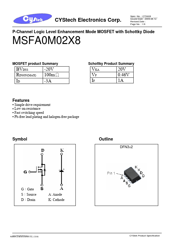
Pb-free lead plating and halogen-free package
Symbol
Outline
DFN3×2
G:Gate S:Source D:Drain
A: Anode K: Cathode
MSFA0M02X8
CYStek Product Specification
CYStech Electronics Corp. Absolute Maximum Ratings (TA=25°C, unless otherwise noted)
Parameter Drain-Source Breakdown Voltage Gate-Source Voltage Continuous Drain Current @TA=25 °C Continuous Drain Current @TA=70 °C Pulsed Drain Current.
The following content is an automatically extracted verbatim text
from the original manufacturer datasheet and is provided for reference purposes only.
View original datasheet text
CYStech Electronics Corp.
Spec. No. : C724X8 www.DataSheet4U.com Issued Date : 2009.06.12 Revised Date : Page No. : 1/9
P-Channel Logic Level Enhancement Mode MOSFET with Schottky Diode
MSFA0M02X8
MOSFET product Summary Schottky Product Summary
BVDSS RDSON(MAX) ID
-20V 100mΩ -3A
VKA VF IF
20V 0.46V 1A
Features
• Simple drive requirement • Low on-resistance • Fast switching speed • Pb-free lead plating and halogen-free package
Symbol
Outline
DFN3×2
G:Gate S:Source D:Drain
A: Anode K: Cathode
MSFA0M02X8
CYStek Product Specification
CYStech Electronics Corp.