Datasheet4U.com
🌙
MTA050P02DFJ6 Datasheet | Cystech Electonics
Part:
MTA050P02DFJ6
Description:
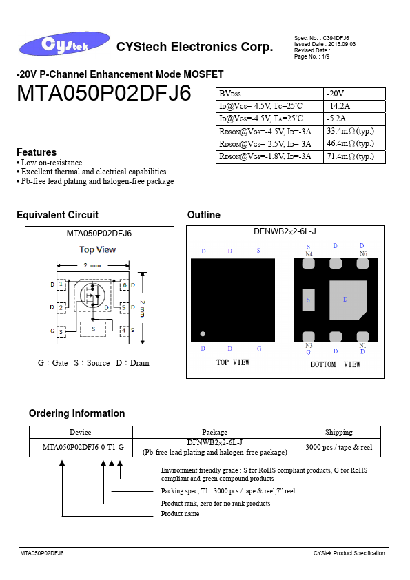
P-Channel Enhancement Mode MOSFET
Category:
MOSFET
Manufacturer:
Cystech Electonics
Size:
418.02 KB
MTA050P02DFJ6 Datasheet (PDF) Download
Cystech Electonics
MTA050P02DFJ6
Key Features
Low on-resistance
Excellent thermal and electrical capabilities
Pb-free lead plating and halogen-free package
×
Close