Cystech BTD5213M3
NPN Planar Transistor
| Part No. | BTD5213M3 |
|---|---|
| Datasheet | BTD5213M3 Download |
| Manufacturer |  Cystech |
| Description | NPN Planar Transistor |
| Buy | Stock & Price |
FEATURES
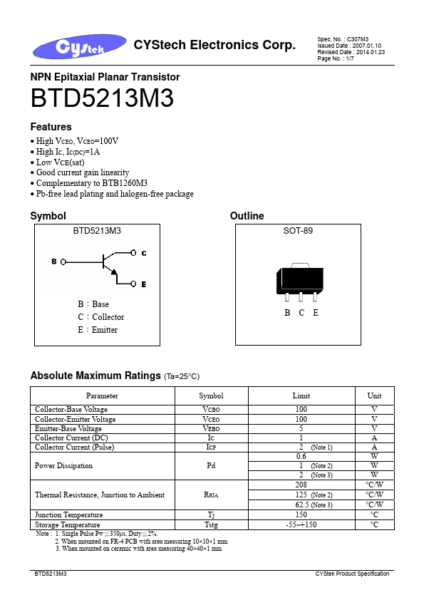
● High VCEO, VCEO=100V● High IC, IC(DC)=1A
● Low VCE(sat)
● Good current gain linearity
● Complementary to BTB1260M3
● Pb-free lead plating and halogen-free package Symbol BTD5213M3 Outline SOT-89 B:Base C:Collector E:Emitter
ABSOLUTE MAXIMUM RATINGS
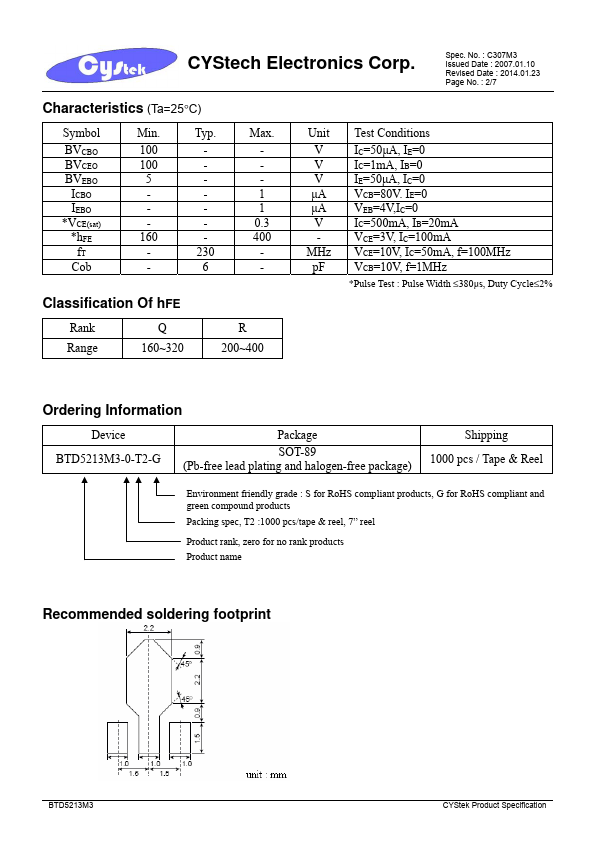
(Ta=25°C) Parameter Collector-Base Voltage Collector-Emitter Voltage Emitter-Base Voltage Collector Current (DC) Collector Current (Pulse) Symbol VCBO VCEO VEBO IC ICP Power Dissipation Pd Thermal Resistance, Junction to Ambient RθJA Junction Temperature Tj Storage Temperature Tstg Note : 1. Single Pulse Pw≦350μs, Duty≦2%. 2. When mounted on FR-4 PCB with area measuring 10×10×1 mm 3. When mounted on ceramic with area measuring 40×40×1 mm BTD5213M3 BCE Limit 100 100 5 1 2 (Note 1) 0.6 1 (Note 2) 2 (Note 3) 208 125 (Note 2) 62.5 (Note 3) 150 -55~+150 Unit V V V A A W W W °C/W °C/W °C/W °C °C CYStek Product Specification CYStech Electronics Corp. Spec. No. : C307M3 Issued Date : 2007.01.10 Revised Date : 2014.01.23 Page No. : 2/7 Characteristics (Ta=25°C) Symbol BVCBO BVCEO BVEBO ICBO IEBO *VCE(sat) *hFE fT Cob Min.