INS6104A
INS6104A is 1:4 Low Skew Clock Buffer manufactured by DAPU.
- 1:4 Low Skew Clock Buffer
Features
- Low skew outputs (50ps)
- Low power CMOS technology
- Operating Voltages of 3.3V/2.5V ± 5%
- Output Enable pin tri-states outputs
- 3.6 V tolerant input clock
- Totally Lead-Free & Fully Ro HS pliant
- Halogen and Antimony Free. “Green” Device
- Industrial temperature range: -40°C to +85°C
- Packaged: 8-pin SOIC
Logic Control
APPLICATIONS
- Wireless BBU, RRU and Wired munication
- Servers, puting, PCI Express (PCIe)
- Switches, Routers, Line Cards, Timing Cards
BUF_IN
数 驭 科 中
GENERAL DESCRIPTIONS
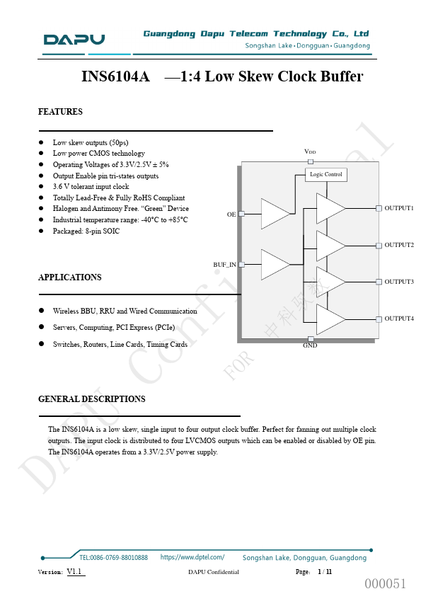
OUTPUT1 OUTPUT2 OUTPUT3 OUTPUT4
The INS6104A is a low skew, single input to four output clock buffer. Perfect for fanning out multiple clock outputs. The input clock is distributed to four LVCMOS outputs which can be enabled or disabled by OE pin. The INS6104A operates from a 3.3V/2.5V power supply.
Version:V1.1
DAPU Confidential
Page: 1 / 11
Version
V1.0 V1.1
Table of Amendment
Revised Content
Draft
First...