INS6110 Overview
Key Specifications
Height: 750 µm
Length: 5 mm
Max Operating Temp: 85 °C
Description
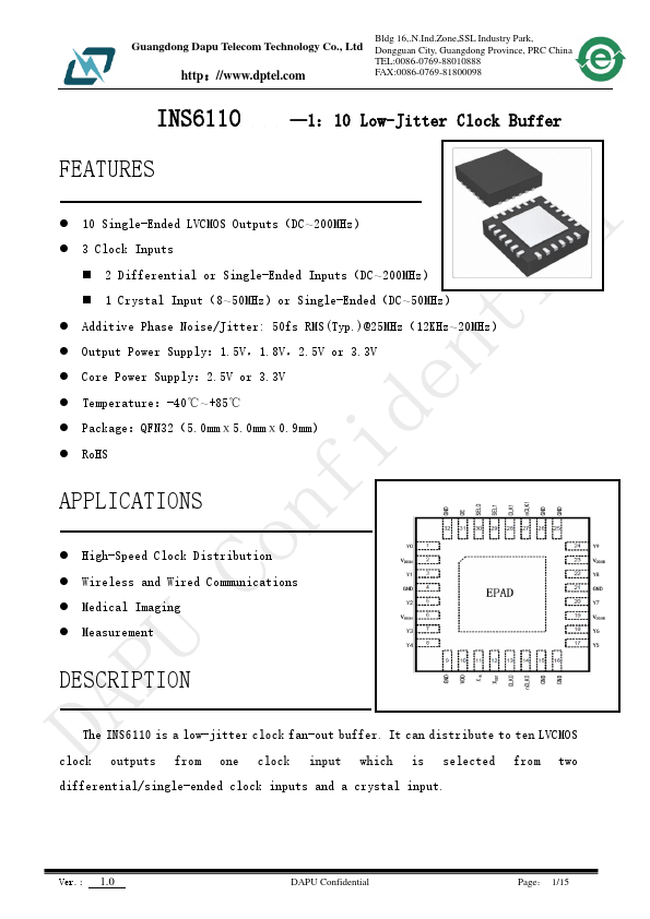
The INS6110 is a low-jitter clock fan-out buffer. It can distribute to ten LVCMOS clock outputs from one clock input which is selected from two differential/single-ended clock inputs and a crystal input.
Key Features
- 10 Single-Ended LVCMOS Outputs(DC~200MHz)
- 3 Clock Inputs
- 2 Differential or Single-Ended Inputs(DC~200MHz)
- 1 Crystal Input(8~50MHz)or Single-Ended(DC~50MHz)
- Additive Phase Noise/Jitter: 50fs RMS(Typ.)@25MHz(12KHz~20MHz)