INS6310A Overview
Key Specifications
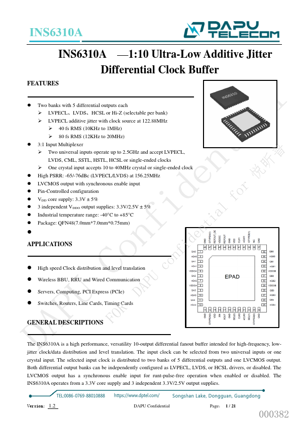
Height: 750 µm
Length: 7 mm
Max Operating Temp: 85 °C
Key Features
- Two banks with 5 differential outputs each
- LVPECL、LVDS、HCSL or Hi-Z (selectable per bank)
- LVPECL additive jitter with clock source at 122.88MHz
- 40 fs RMS (10KHz to 1MHz)
- 80 fs RMS (12KHz to 20MHz)