Datasheet Summary
14-Bit, 250MSPS, Low-Power D/A Converters
Features n 14-Bit resolution n 250MSPS conversion rate n 2mA -20mA output current n Operates from single +2.7 to +3.6 Volt supply n Low power, 120mW n Internal +1.24 Volt reference
- optional external reference n Outstanding dynamic performance n Guaranteed monotonicity n Humidity and stress resistant ceramic LCC package for -QL and /883 models n -40°C to +105°C and -55°C to +125°C operating temperature ranges n 100% testing over temperature n )JHI3FMQSPDFTTøPXCVSOJOFOWJSPONFOUBMMPU and ATE traceability n 28 pin TSSOP package (SE, SM) n Pb-free RoHS pliant
PRODUCT OVERVIEW
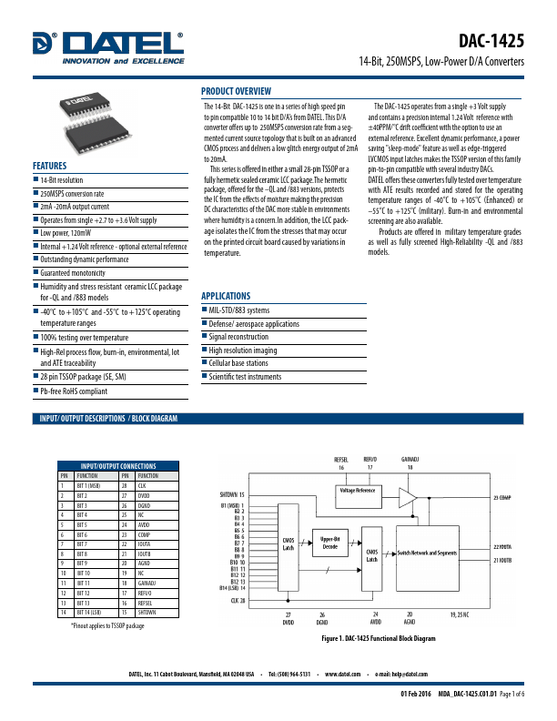
The 14-Bit DAC-1425 is one in a series of high...