B507
Description
Designed for use in power amplifier and switching circuits.
Pinning
1 = Base 2 = Collector 3 = Emitter
Absolute Maximum Ratings(TA=25o C)
Characteristic Collector-Base Voltage Collector-Emitter Voltage Emitter-Base Voltage Collector Current Total Power Dissipation Total Power Dissipation(TC=25o C) Junction Temperature Storage Temperature
Symbol VCBO VCEO VEBO IC PD PD TJ TSTG
Rating Unit
-60
-60
-5
-3
+150 o C
-55 to +150 o C
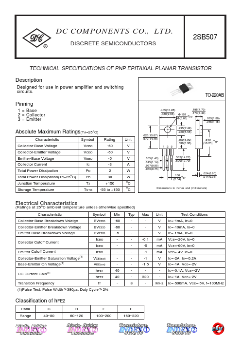
TO-220AB
.405(10.28)
.185(4.70)
.380(9.66)
Φ.151 Φ(3.83)
.173(4.40) Typ
.055(1.39)
.045(1.15)
.625(15.87) .570(14.48)
.295(7.49) .220(5.58)
.350(8.90) .330(8.38)
.640 (16.25)
Typ
.055(1.40) .045(1.14) .037(0.95) .030(0.75)
.562(14.27) .500(12.70)
.100 (2.54)
Typ
.024(0.60) .014(0.35)
Dimensions in inches and (millimeters)
Electrical Characteristics
(Ratings at 25o C ambient temperature unless otherwise...