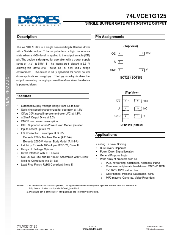
74LVCE1G125 Description
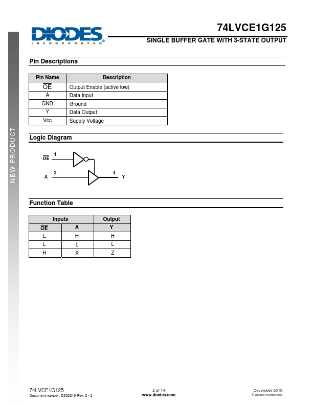
The 74LVCE1G125 is a single non-inverting buffer/bus driver with a 3-state output. T he out put enters a high impedance state when a HIGH-level is applied to the output en able (OE) pin. The device is designed for operation with a power supply range of 1.4V to 5.5V.