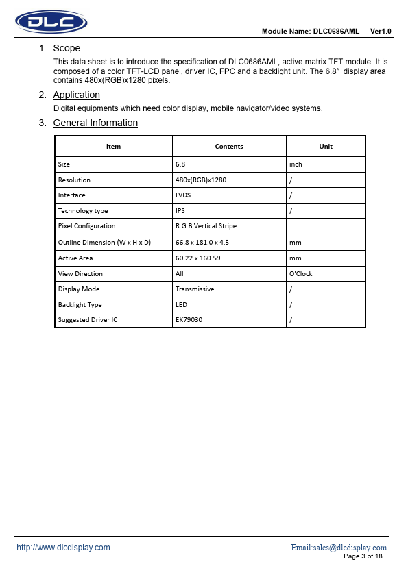
DESCRIPTION
Common voltage Power supply Power supply No connection Global reset pin. Standby mode Power Ground Differential Data Input ,CH0(Negative) Differential Data Input ,CH0(Positive) Power Ground Differential Data Input ,CH1(Negative) Differential Data Input ,CH1(Positive) Power Ground Differential Data Input ,CH2(Negative) Differential Data Input ,CH2(Positive) Power Ground Differential Clock Input Negative) Differential Clock Input ((Positive) Power Ground Differential Data Input ,CH3(Negative) Differential Data Input ,CH3(Positive) Power Ground No connection No connection Power Ground No connection No connection In LVDS interface connected HSD to FPC for Pin Setting HSD=”L”:8 bit; HSD=”H”:6 bit Power supply for analog circuits Power Ground No connection No connection Source Right or Left sequence control. Gate Up or Down scan control. Gate OFF Voltage No connection No connection Gate ON Voltage No connection No connection Remark Ver1.0 Email:sales@dlcdisplay.com Page 5 of 18 6.