DP3S1MX32PY5
DP3S1MX32PY5 is 32M CMOS SRAM manufactured by DPAC Technologies.
DESCRIPTION
:
The DP3S1MX32PY5 is a 1M x 32 SRAM module that utilizes the new and innovative space saving TSOP stacking technology. The module is constructed of two 1M x 16 SRAM’ s that are configured as a 1M x 32. The DP3S1MX32PY5 module features high speed access times with mon data inputs and outputs.
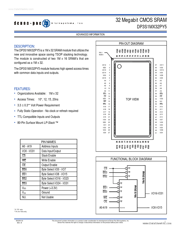
PIN 1 INDEX
PIN-OUT DIAGRAM
FEATURES
:
- Organizations Available: 1M x 32
- Access Times: 10- , 12, 15, 20ns
- 3.3 ±0.3-
- Volt Power Requirement
- Fully Static Operation
- No clock or refresh required
- TTL-patible Inputs and Outputs
- 80-Pin Surface Mount LP-Stack ™
I/O12 VDD I/O13 I/O14 VSS I/O15 A4 A3 A2 A1 A0 BS1 CS VDD WE BS3 A19 A18 A17 A16 A15 I/O0 VDD I/O1 I/O2 VSS I/O3
1 2 3 4 5 6 7 8 9 10 11 12 13 14 15 16 17 18 19 20 21 22 23 24 25 26 27
TOP VIEW
67 66 65 64 63 62 61 60 59 58 57 56 55 54 53 52 51 50 49 48 47 46 45 44 43 42 41
I/O11 VSS I/O10 I/O9 VDD I/O8 A5 A6 A7 A8 A9 BS2 OE VSS NU BS0 A10 A11 A12 A13 A14 I/O7 VSS I/O6 I/O5 VDD I/O4
PIN NAMES
A0
- A19 I/O0
- I/O31 CS WE OE BS0 BS1 BS2 BS3 VDD VSS NU. Address Inputs Data Input/Output Stack Enable Write Enable Output Enable Byte Select I/O0
- I/O7 Byte Select I/O8
- I/O15 Byte Select I/O16
- I/O23 Byte Select I/O24
- I/O31 Power (+3.3V) Ground Not Usable
BS1 BS0 WE OE A0-A19 CS BS3 BS2
CE UB LB WE OE A0-A19 CE UB LB
FUNCTIONAL BLOCK DIAGRAM
I/O16-I/O31
- 0°-70° only.
- - 5% for 10ns only.
I/O0-I/O15
30A244-00 REV. B
This document contains information on a product under consideration for development at Dense-Pac Microsystems, Inc. Dense-Pac reserves the right to change or discontinue information on this product without prior notice.
..
ADVANCED...