FEATURES
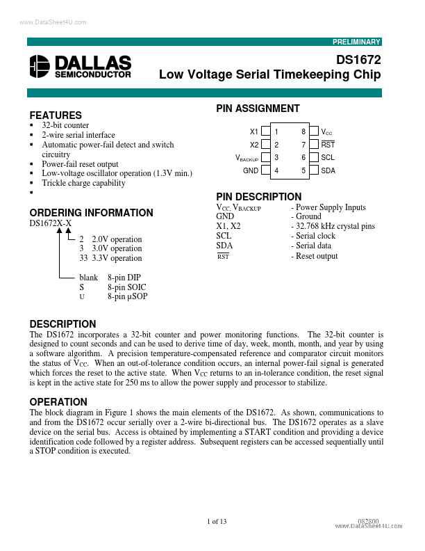
32-bit counter 2-wire serial interface Automatic power-fail detect and switch circuitry Power-fail reset output Low-voltage oscillator operation (1.3V min.) Trickle charge capability PIN ASSIGNMENT X1 X2 VBACKUP GND 1 2 3 4 8 7 6 5 VCC RST SCL SDA PIN DESCRIPTION
ORDERING INFORMATION DS1672X-X 2 2.0V operation 3 3.0V operation 33 3.3V operation blank S U VCC, VBACKUP GND X1, X2 SCL SDA RST - Power Supply Inputs - Ground - 32.768 kHz crystal pins - Serial clock - Serial data - Reset output 8-pin DIP 8-pin SOIC 8-pin µSOP DESCRIPTION
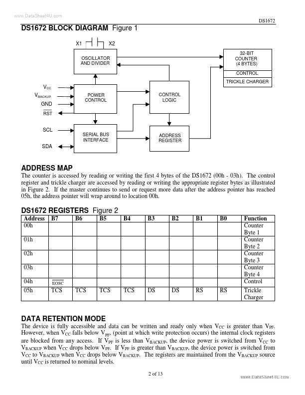
A precision temperature-compensated reference and comparator circuit monitors the status of VCC. When VCC returns to an in-tolerance condition, the reset signal is kept in the active state for 250 ms to allow the power supply and processor to stabilize. OPERATION The block diagram in Figure 1 shows the main elements of the DS1672. As shown, communications to and from the DS1672 occur serially over a 2-wire bi-directional bus. The DS1672 operates as a slave device on the serial bus. Dallas Semiconductor