Data Delay Devices PDU16F
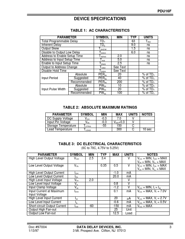
The PDU16F is a memory device. The timing restrictions are shown in Figure 1. This time is given by the following relation: TOAX = max { (Ai - A i-1) * TINC , 0 } where A i-1 and Ai are the old and new address codes, respectively.| Part No. | PDU16F |
|---|---|
| Datasheet | PDU16F Download |
| Manufacturer |  Data Delay Devices |
| Description | 6-BIT PROGRAMMABLE DELAY LINE |
| Buy | Stock & Price |
FEATURES
●●
●
●
●
●
●
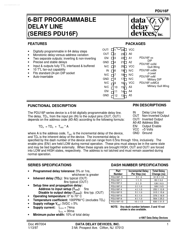
● Digitally programmable in 64 delay steps Monotonic delay-versus-address variation Two separate outputs: inverting & non-inverting Precise and stable delays Input & outputs fully TTL interfaced & buffered 10 T2L fan-out capability Fits standard 24-pin DIP socket Auto-insertable OUT/ OUT EN/ GND N/C IN N/C GND N/C N/C EN/ GND 1 2 3 4 5 6 7 8 9 10 11 12 24 23 22 21 20 19 18 17 16 15 14 13 data 3 ® delay devices, inc. PACKAGES VCC A0 A1 A2 VCC N/C N/C N/C VCC A3 A4 A5 PDU16F-xx DIP PDU16F-xxA4 Gull-Wing PDU16F-xxB4 J-Lead PDU16F-xxM Military DIP PDU16F-xxMC4 Military Gull-Wing FUNCTIONAL
DESCRIPTION
The PDU16F-series device is a 6-bit digitally programmable delay line. The delay, TDA, from the input pin (IN) to the output pins (OUT, OUT/) depends on the address code (A5-A0) according to the following formula: TDA = TD0 + TINC * A PIN DESCRIPTIONS IN OUT OUT/ A0-A5 EN/ VCC GND Delay Line Input Non-inverted Output Inverted Output Address Bits Output Enable +5 Volts Ground where A is the address code, TINC is the incremental delay of the device, and TD0 is the inherent delay of the device.