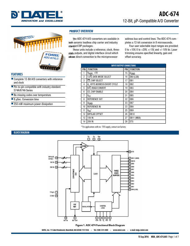
FEATURES
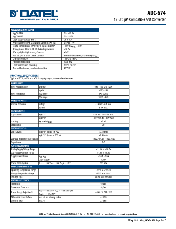
n Complete 12-Bit A/D converters with reference and clock n Pin-to-pin compatible with industry standard 574A/674A Series n No missing codes over temperature n ç4FD $POWFSTJPO UJNF n 250 mW maximum power dissipation BLOCK DIAGRAM INPUT/OUTPUT CONNECTIONS PIN FUNCTION 1 Vlogic, +5V 2 12/8, DATA MODE SELECT PIN FUNCTION 15 DGND 16 DB0 (LSB) 3 CS, CHIP SELECT 17 DB1 4 A0, BYTE ADDRESS/SHORT CYCLE 5 R/C, READ/CONVERT 18 DB2 19 DB3 6 CE, CHIP ENABLE 20 DB4 7 Vcc 8 REFERENCE OUT 21 DB5 22 DB6 9 AGND 10 REFERENCE IN 23 DB7 23 DB8 11 Vee* 12 BIPOLAR OFFSET 25 DB9 26 DB10 13 10V IN 27 DB11 (MSB) 14 20V IN 28 STS * For applications with no -15V supply, contact our factory. Figure 1. ADC-674 Functional Block Diagram %"5&- *OD $BCPU #PVMFWBSE .BOTö FME ." 64" t 5FM t XXX EBUFM DPN t F NBJM IFMQ!EBUFM DPN 15 Sep 2016 MDA_ADC-674.A03 Page 1 of 7 ADC-674 #JU ç1 $PNQBUJCMF " % $POWFSUFS ABSOLUTE MAXIMUM RATINGS
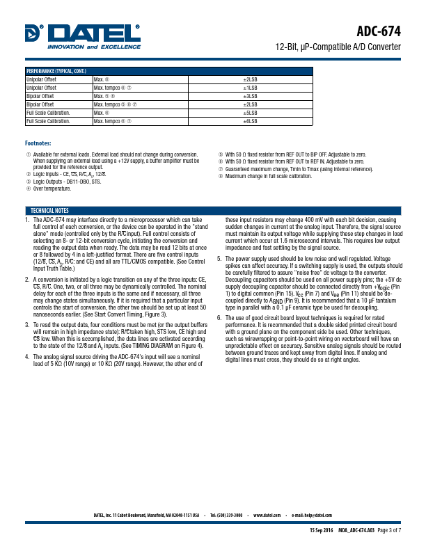
Vcc TO GND Vee TO GND Logic Supply Voltage (Pin 1) Analog Common (Pin 9) to Digita... Datel