MID112 Overview
Description
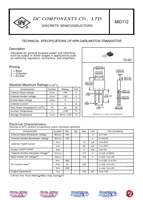
Designed for general purpose power and switching such as output or driver stages in applications such as switching regulators, converters, and amplifiers. TO-251 .268(6.80) .252(6.40) .217(5.50) .205(5.20) 2 Pinning 1 = Base 2 = Collector 3 = Emitter .022(0.55) .018(0.45) .063(1.60) .055(1.40) Characteristic Collector-Base Voltage Collector-Emitter Voltage Emitter-Base Voltage Collector Current Total Power Dissipation(TC=25 C) Junction Temperature Storage Temperature o .284(7.20) .268(6.80) Symbol VCBO VCEO VEBO IC PD TJ TSTG Rating 100 100 5 2 20 +150 -55 to +150 Unit V V V A W o o .032 Max (0.80) .035 Max (0.90) 1 2 3 .059(1.50) .035(0.90) .256 Min (6.50) .024(0.60) .018(0.45) .181 Typ (4.60) .095(2.40) .087(2.20) C Dimensions in inches and (millimeters) C Characteristic (Ratings at 25 C ambient temperature unless otherwise specified) Symbol BVCBO BVCEO ICBO ICEO IEBO VCE(sat) VBE(on) hFE1 hFE2 hFE3 Cob 380µs, Duty Cycle 2% Min 100 100 500 1K 200 - Typ - Max 10 20 2 2.5 2.8 12K 100 Unit V V µA µA mA V V pF IC=1mA Test Conditions IC=30mA VCB=80V VCE=50V VBE=5V IC=2A, IB=8mA IC=2A, VCE=3V IC=0.5A, VCE=3V IC=2A, VCE=3V IC=4A, VCE=3V VCB=10V Collector-Base Breakdown Voltage Collector-Emitter Breakdown Voltage Collector Cutoff Current Emitter Cutoff Current Collector-Emitter Saturation Voltage(1) Base-Emitter On Voltage(1) DC Current Gain(1) Output Capacitance (1)Pulse Test: Pulse Width.