74AHC125S14 Overview
Key Specifications
Package: SOP
Mount Type: Surface Mount
Pins: 14
Operating Voltage: 3.3 V
Description
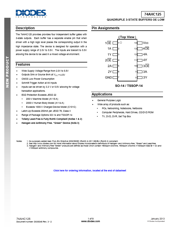
The 74AHC125 provides provides four independent buffer gates with 3-state outputs. Each buffer has a separate enable pin that when driven with a high logic level places the corresponding output in the high impedance state.
Key Features
- Wide Supply Voltage Range from 2.0V to 5.5V
- Outputs Sink or Source 8mA at VCC = 4.5V
- CMOS Low Power Consumption
- Schmitt Trigger Action at All Inputs
- Inputs can be driven by 3.3 V or 5.5V allowing for voltage translation applications