74AUP2G125
74AUP2G125 is DUAL 3-STATE BUFFER manufactured by Diodes Incorporated.
NEW PRODUCT
DUAL 3-STATE BUFFER
Description
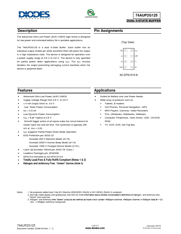
Pin Assignments
The Advanced Ultra Low Power (AUP) CMOS logic family is designed for low power and extended battery life in portable applications.
The 74AUP2G125 is a dual 3-State Buffer. Each buffer has an individual output enable pin while asserted HIGH will place the output in a high impedance state. The device is designed for operation over a power supply range of 0.8 V to 3.6 V. The device is fully specified for partial power down applications using IOFF. The IOFF circuitry disables the output preventing damaging current backflow when the device is powered down.
(Top View)
X2-DFN1210-8
Features
- Advanced Ultra Low Power...