74HCT126
74HCT126 is QUADRUPLE 3-STATE BUFFERS manufactured by Diodes Incorporated.
QUADRUPLE 3-STATE BUFFERS OE HIGH
Description
The 74HCT126 provides provides four independent buffer gates with 3-state outputs. Each buffer has a separate enable pin that if driven with a low logic level places the corresponding output in the high impedance state. The device is designed for operation with a power supply range of 4.5V to 5.5V.
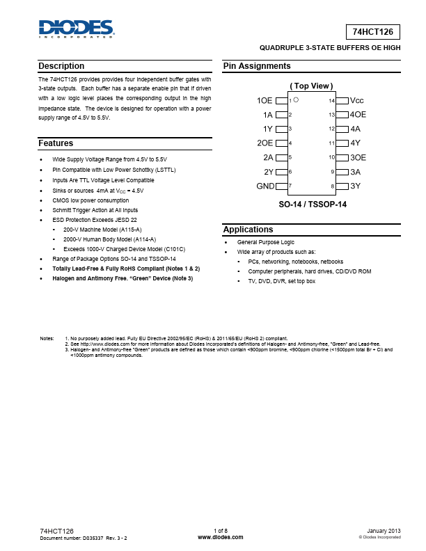
Pin Assignments
Features
- Wide Supply Voltage Range from 4.5V to 5.5V
- Pin patible with Low Power Schottky (LSTTL)
- Inputs Are TTL Voltage Level patible
- Sinks or sources 4mA at VCC = 4.5V
- CMOS low power consumption
- Schmitt Trigger Action at All Inputs
- ESD Protection Exceeds JESD 22
- 200-V Machine Model (A115-A)
- 2000-V...