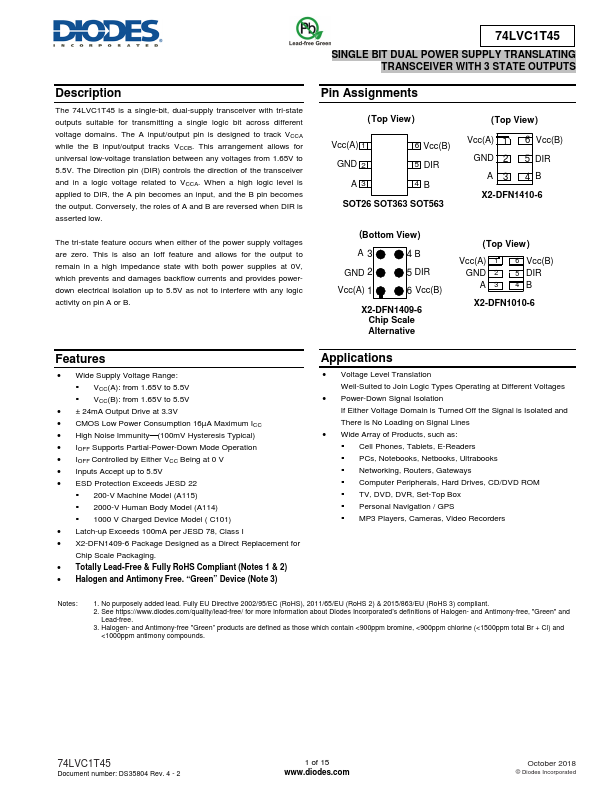
74LVC1T45
Description
The 74LVC1T45 is a single-bit, dual-supply transceiver with tri-state outputs suitable for transmitting a single logic bit across different voltage domains.
Key Features
- Wide Supply Voltage Range
- VCC(A): from 1.65V to 5.5V
- VCC(B): from 1.65V to 5.5V
- ± 24mA Output Drive at 3.3V
- CMOS Low Power Consumption 16µA Maximum ICC
- High Noise Immunity(100mV Hysteresis Typical)
- IOFF Supports Partial-Power-Down Mode Operation
- IOFF Controlled by Either VCC Being at 0 V
- Inputs Accept up to 5.5V
- ESD Protection Exceeds JESD 22
Applications
- Power-Down Signal Isolation If Either Voltage Domain is Turned Off the Signal is Isolated and There is No Loading on Signal Lines