AP22913
AP22913 is SINGLE SLEW RATE CONTROLLED LOAD SWITCH manufactured by Diodes Incorporated.
SINGLE SLEW RATE CONTROLLED LOAD SWITCH
Description
The AP22913 slew rate controlled load switch is a single P-channel MOSFET power switch designed for high-side load-switching applications. The MOSFET has a typical RDS(on) of 54mΩ at 5V (X1WLB0909-4), allowing increased load current handling capacity with a low forward voltage drop. The turn-on slew rate of the device is controlled internally. VIN and VOUT are isolated during the OFF state with a TRCB (True Reverse Current Blocking) feature.
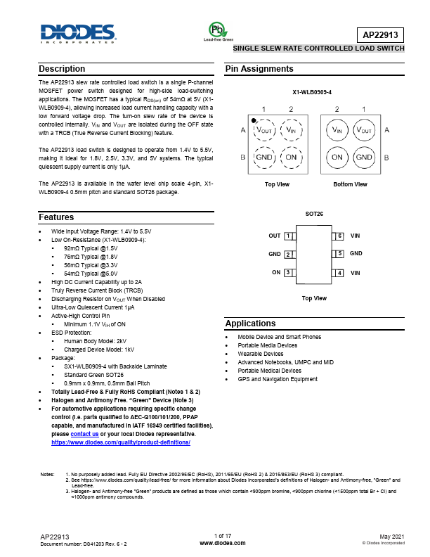
Pin Assignments
X1-WLB0909-4
The AP22913 load switch is designed to operate from 1.4V to 5.5V, making it ideal for 1.8V, 2.5V, 3.3V, and 5V systems. The typical quiescent supply current is only 1µA.
The AP22913 is available in the wafer level chip scale 4-pin, X1WLB0909-4 0.5mm pitch and standard SOT26 package.
Top View
Bottom View
Features
- Wide Input Voltage Range: 1.4V to 5.5V
- Low On-Resistance (X1-WLB0909-4):
- 92mΩ Typical @1.5V
- 76mΩ Typical @1.8V
- 56mΩ Typical @3.3V
- 54mΩ Typical @5.0V
- High DC Current Capability up to 2A
- Truly Reverse Current Block (TRCB)
- Discharging Resistor on VOUT When Disabled
- Ultra-Low Quiescent Current 1µA
- Active-High Control Pin
- Minimum 1.1V VIH of ON
- ESD Protection:
- Human Body Model: 2k V
- Charged Device Model: 1k V
- Package:
- SX1-WLB0909-4 with Backside Laminate
- Standard Green SOT26
- 0.9mm x 0.9mm, 0.5mm Ball Pitch
- Totally Lead-Free & Fully Ro HS pliant (Notes 1 &...