DMC1030UFDB
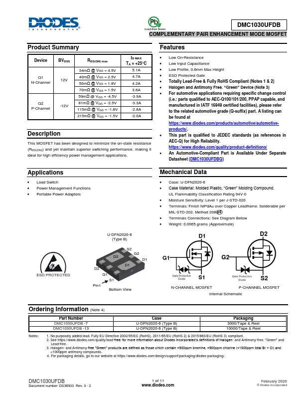
Description
This MOSFET has been designed to minimize the on-state resistance (RDS(ON)) and yet maintain superior switching performance, making it ideal for high efficiency power management applications.
Key Features
- Low On-Resistance
- Low Input Capacitance
- Low Profile, 0.6mm Max Height
- ESD Protected Gate
- Totally Lead-Free & Fully RoHS pliant (Notes 1 &
- Halogen and Antimony Free. “Green” Device (Note
- This part is qualified to JEDEC standards (as references in AEC-Q) for High Reliability. https://.diodes./quality/product-definitions/
- An Automotive-pliant Part is Available Under Separate Datasheet (DMC1030UFDBQ)