Click to expand full text
ADAVDAVNAECNEWCDEPI IRNNOFFDOOURRCMTMAATITIOONN
DMC25D1UVT
COMPLEMENTARY PAIR ENHANCEMENT MODE MOSFET
Product Summary
Device Q1 Q2
V(BR)DSS 25V -12V
RDS(ON)
4Ω @ VGS = 4.5V 55mΩ @ VGS= -4.5V 70mΩ @ VGS= -2.5V
ID TA = +25°C
0.5A
-3.9A
-3.5A
Description
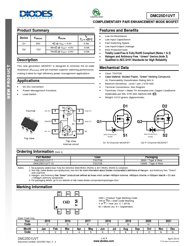
This new generation MOSFET is designed to minimize the on-state resistance (RDS(ON)) and yet maintain superior switching performance, making it ideal for high efficiency power management applications.
Applications
DC-DC Converters Power Management Functions Load Switch
Features and Benefits
Low On-Resistance Low Input Capacitance Fast Switching Speed Low Input/Output Leakage ESD Protected Gate Totally Lead-Free & Fully RoHS Compliant (Notes 1 & 2) Halogen and Antimony Free.