DMC2990UDJQ
Description
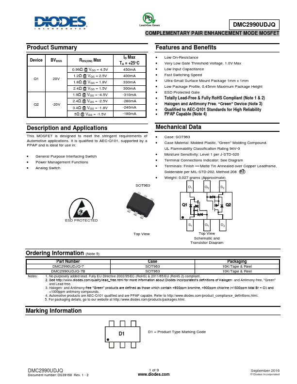
and Applications Mechanical Data This MOSFET is designed to meet the stringent requirements of Automotive app.
Key Features
- Halogen and Antimony Free. “Green” Device (Note
- Qualified to AEC-Q101 Standards for High Reliability PPAP Capable (Note 4)