Download DMP1018UCB9 Datasheet PDF
DMP1018UCB9 page 2
Page 2
DMP1018UCB9 page 3
Page 3

DMP1018UCB9 Description

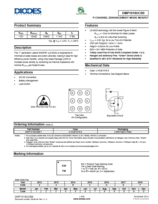
This 1st generation Lateral MOSFET (LD-MOS) is engineered to minimize on-state losses and switch ultra-fast, making it ideal for high efficiency power transfer. Using Chip-Scale Package (CSP) to increase power density by bining low thermal impedance with minimal RDS(on) per footprint area. Applications  DC-DC Converters  Battery Management  Load Switch DMP1018UCB9 P-CHANNEL ENHANCEMENT MODE MOSFET.

DMP1018UCB9 Key Features

  • LD-MOS technology with the lowest Figure of Merit: RDS(on) = 12mΩ to Minimize On-State Losses Qg = 4.9nC for Ultra-Fast
  • Vgs(th) = -0.8V typ. for a Low Turn-On Potential
  • CSP with Footprint 1.5mm × 1.5mm
  • Height = 0.62mm for Low Profile
  • ESD = 3kV HBM Protection of Gate
  • Totally Lead-Free & Fully RoHS pliant (Notes 1 & 2)
  • Halogen and Antimony Free. “Green” Device (Note 3)
  • Qualified to AEC-Q101 Standards for High Reliability
  • Case: U-WLB1515-9
  • Terminal Connections: See Diagram Below