DMP2540UCB9
Description
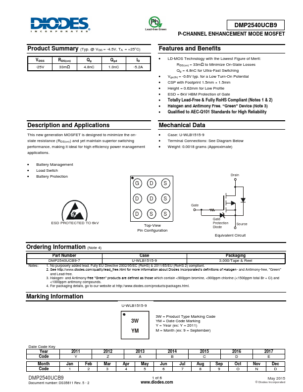
and Applications This new generation MOSFET is designed to minimize the onstate resistance (RDS(on)) and yet maintain superior switching performance, making it ideal for high efficiency power management applications.
Key Features
- Halogen and Antimony Free. “Green” Device (Note
- Qualified to AEC-Q101 Standards for High Reliability