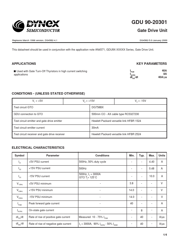
GDU90-20301
GDU90-20301 is Gate Drive Unit manufactured by Dynex Semiconductor.
GDU 90 20301
GDU 90-20301
Gate Drive Unit
Replaces March 1998 version, DS4562-4.1 DS4562-5.0 January 2000
This datasheet should be used in conjunction with the application note AN4571, GDU9X-XXXXX Series, Gate Drive Unit.
APPLICATIONS s Used with Gate Turn-Off Thyristors in high current switching applications
KEY PARAMETERS
IFGM IG(ON) d IGQ/dt 40A 8A 40A/µs
CONDITIONS
- (UNLESS STATED OTHERWISE)
V1 = +5V Test circuit GTO GDU connection to GTO Test circuit emitter and gate drive emitter Test circuit emitter current Test circuit receiver and gate drive receiver V2 = +15V DG758BX 500mm CO
- AX cable type RC5327230 Hewlett Packard versatile link HFBR 1524 30m A Hewlett Packard versatile link HFBR 2524 V3 = -15V
ELECTRICAL CHARACTERISTICS
Symbol IV1 IV2 IV3 V1(Min) V2(Min) V3(Min) IFGM IG(ON) d IFG/dt d IGQ/dt Parameter +5V PSU current +15V PSU current -15V PSU current +5V PSU minimum +15V PSU minimum -15V PSU minimum Peak forward gate current On-state gate current Rate of rise of positive gate current Rate of rise of negative gate current Conditions 500Hz, 50% duty cycle 500Hz 500Hz, IT = 3000A GTO Tj= 125˚C Min. Typ. Max. 4.40 0.48 10.0 Units A A A V V V A A A/µs A/µs
3.8 14.0 14.0 40
8 40 40
Measured 10
- 75% IFGM IT = 3000A, 90% IG(ON)
- 50% IGQM
- -
1/4
GDU 90 20301
TIMING CHARACTERISTICS
Symbol t1- † t2 t3- † t4 t5- t6 t7 t8- t9 t10 t11 t12 Parameter No response pulse width of input signal Delay time emitter current to receiver o/p Turn-on delay emitter current to 10% IFGM IFGM pulse width Minimum on time 10% IFGM to 90% IG(ON) Receiver storage time Turn-off delay. Emitter current to 90% IG(ON) Minimum off time 90% IG(ON) to 10% IFGM Delay time Gate volts to o/p emitter current Turn-off delay Gate volts to test receiver o/p Storage time Gate volts to o/p emitter current Turn-on delay Gate volts to test receiver o/p
†
Conditions Adjustable by R81 + R82
Min. 2 0.2 5.0
Typ.
Max. 3 0.4 5.8
Units µs µs µs µs µs µs µs µs µs µs µs µs
Adjustable by...