EDI8M1664C100
EDI8M1664C100 is Megabit SRAM Module manufactured by EDI.
- Part of the EDI8M1664C50 comparator family.
- Part of the EDI8M1664C50 comparator family.
~EDI
64Kx16 Static RAM CMOS, Module
EDI8M1664C501601701851100
Megabit SRAM Module, JEDEC Pinout
Features
The EDI8M1664C isa high speed 64Kx16 CMOS Static 64Kx16 bit CMOS Static
RAM Module consisting of four (4) 32Kx8 CMOS Static Random Access Memory Module
RAMs in leadless chip carriers, surface mounted onto a
- Access Times 50, 60, 70, 85, and 100ns mu~i-Iayered ceramic substrate. The 32Kx8 RAMs are
- Fully Static, No Clocks organized as two banks of 32Kx16 bits each. Functional
- Inputs and Outputs Directly TTL patible equivalence to proposed monolithic megabit Static
- Data Retention Function
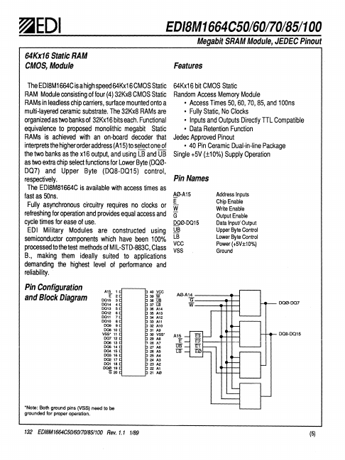
RAMs is achieved with an on-board decoder that Jedec Approved Pinout interprets the higherorderaddress (A15)to select one of
- 40 Pin Ceramic Dual-in-line Package the two banks as the x16 output, and using LB and UB Single +5V (±10%) Supply Operation as two extra chip select functions for Lower Byte (000-
007) and Upper Byte (008-0015) control, respectively.
Pin Names
The EDI8M81664C is available with access times as fast as SOns.
Fully asynchronous circuitry requires no clocks or refreshing for operation and provides equal access and cycle times for ease of use.
~0-A15
000-0015
Address Inputs Chip Enable Write Enable Output Enable Data Input! Output
EDI Military Modules are constructed using semiconductor ponents which have been 100% processedtothetest methods of Mll-STD-883C, Class B., making them ideally suited to applications
UB LB VCC VSS
Upper Byte Control Lower Byte Control Power (+5V±10%) Ground demanding the highest level of performance and reliability.
Pin Configuration and Block Diagram
Al~ 1 [
E 0015
~3~~
0014 ~ [
0013 5...