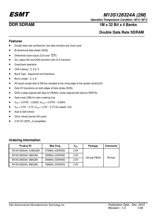
Datasheet4U Logo Datasheet4U.com

M13S128324A - Double Data Rate SDRAM

Description

DM is an input mask signal for write data.

Features

  • Double-data-rate architecture, two data transfers per clock cycle.
  • Bi-directional data strobe (DQS).
  • Differential clock inputs (CLK and CLK ).
  • DLL aligns DQ and DQS transition with CLK transition.
  • Quad bank operation.
  • CAS Latency : 2, 2.5, 3.
  • Burst Type : Sequential and Interleave.
  • Burst Length : 2, 4, 8.
  • All inputs except data & DM are sampled at the rising edge of the system clock(CLK).
  • Data I/O transitions on both edges of data strobe (DQS).

📥 Download Datasheet

Datasheet Details

Part number M13S128324A
Manufacturer ESMT
File Size 1.72 MB
Description Double Data Rate SDRAM
Datasheet download datasheet M13S128324A Datasheet
Other Datasheets by ESMT

Full PDF Text Transcription

Click to expand full text
ESMT DDR SDRAM M13S128324A (2M) Operation Temperature Condition -40°C~85°C 1M x 32 Bit x 4 Banks Double Data Rate SDRAM Features  Double-data-rate architecture, two data transfers per clock cycle  Bi-directional data strobe (DQS)  Differential clock inputs (CLK and CLK )  DLL aligns DQ and DQS transition with CLK transition  Quad bank operation  CAS Latency : 2, 2.5, 3  Burst Type : Sequential and Interleave  Burst Length : 2, 4, 8  All inputs except data & DM are sampled at the rising edge of the system clock(CLK)  Data I/O transitions on both edges of data strobe (DQS)  DQS is edge-aligned with data for READs; center-aligned with data for WRITEs  Data mask (DM) for write masking only  VDD = 2.375V ~ 2.625V, VDDQ = 2.375V ~ 2.625V  VDD = 2.5V ~ 2.7V, VDDQ = 2.5V ~ 2.
Published: |